Transmission electron microscopy
Transmission electron microscopy (TEM) is an essential technique for understanding the growth mechanisms of materials, enabling their microstructure to be visualized at different scales ranging from micrometers (µm) to the atomic scale. In 2022, the CRHEA, through the ACT-M consortium, acquired a latest-generation transmission electron microscope (TEM) from the ThermoFisher range, a TITAN SPECTRA 200 offering ultimate performance in terms of spatial resolution, 70pm at 200kV, and high energy sensitivity (solid angle: 1.8sr).
More details about the TEM and other equipment on the ACT-M platform can be found at the following link: https://www.crhea.cnrs.fr/ACT-M/
At CRHEA, the MET has two missions:
- A service mission concerning the structural and microstructural characterization of epitaxial materials at CRHEA. This includes conventional measurements for films :
- Analysis of structural defects (measurement of their densities, determination of their nature, etc.)
- Precise measurement of the thickness, composition, and morphology of heterostructures ranging in size from micrometers to nanometers
- Research activity focused on understanding the microstructure of heteroepitaxial thin films as a function of their growth conditions within the framework of various collaborative projects established at the local, national, and international levels
Study of crystalline defects (plane view)
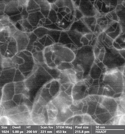 HRSTEM-HAADF image / plane view image illustrating the presence of two types of curved and linear
defects (antiphase boundaries) in a layer of Fe3O4 deposited by PLD.
HRSTEM-HAADF image / plane view image illustrating the presence of two types of curved and linear
defects (antiphase boundaries) in a layer of Fe3O4 deposited by PLD.
Auteurs: I. Madaci, C. Morhain, I. Florea, P. Vennéguès
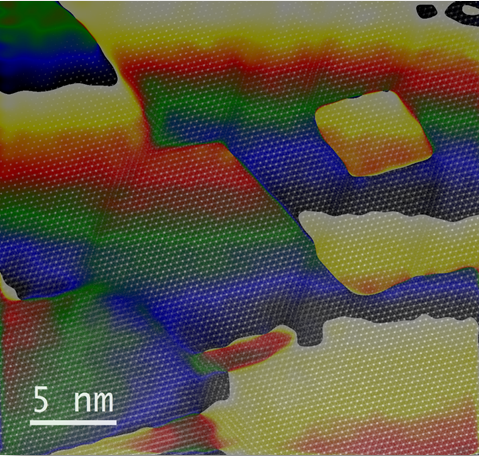
HRSTEM-HAADF image / GPA phase in plane view illustrating the presence of antiphase boundaries (APBs) in a Fe3O4 layer deposited by PLD. Demonstration of direct single-crystal growth of Fe3O4/ZnO, determination of epitaxy relationships, and characterization of APBs.
Auteurs: I. Madaci, C. Morhain, I. Florea, P. Vennéguès
Study of 2D material/substrate interfaces, III-N,…
HRSTEM-HAADF image illustrating the presence of three layers of MoS2 grown by MBE on a GaN substrate. Demonstration of direct single-crystal growth of MoS2/GaN, determination of epitaxial relationships
Auteurs: M. Al Khalfioui, M. T. Dau, I. Florea, P. Vennéguès

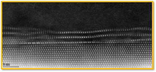
Top: HRSTEM-HAADF image illustrating the presence of a 5nm layer of Nb-N deposited by MBE on an AlN/Si substrate.
Demonstration of direct single crystal growth Nb-N /AlN determination of epitaxy relationships
Bottom: RGB of inverse images calculated by selecting the plane families illustrated by the circles in the FFT image