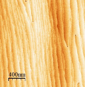
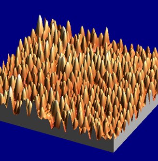
The operating principle of the atomic force microscope (AFM) is to image the surface of a material, from the micrometer to the nanometer scale, via forces of interaction between the atoms of the surface of the sample and the atoms of the tip of the microscope. More precisely, it is a combination between the Van Der Waals attractive forces and coulombian repulsive forces, with a silicon tip, since these microscopes are mainly used in tapping mode. The image obtained makes it possible to determine roughness of the surface, identify and quantify dislocations through1, to measure the dimensions of the atomic steps2 and nanostructures such as quantum dots3.
1) 2D topographic image of the surface of a GaN layer (0001) epitaxied on sapphire (0001)
The dislocations are linear faults which cross the GaN layer from the interface between the GaN and sapphire to the surface. They correspond to non-radiative recombination centers for electrons and holes and thus mitigate the optical efficiency LEDs based on GaN. Observed dislocations (2 edges and 6 mixed) are represented by dots blacks on the AFM image are represented respectively the one hand by the small black holes and the other hand by the big black holes at the intersection of the double atomic steps.

2) 2D topographic image of the surface of a graphene layer epitaxied by CVD on 6H-SiC
Under graphene, the steps of the 6H-SiC substrate can be distinguished from height multiple of that of a Si-C bilayer, 0.25 nm. Most are triple steps of (0.75 nm high, indicated 3 Si-C), but there are also double steps (0.50 nm high, indicated 2 Si-C) or single (0.25 nm high, indicated 1 Si-C). The presence a second layer of graphene, indicated in dotted line, is revealed by the phase image (on the right) and by steps of a height of about 0.35 nm (indicated 2 G). In the frame of collaboration with the Laboratoire National d’Essai et de métrologie (LNE), this type of graphene is used to realize electrical resistance standards based on the quantum Hall effect.

3) 3D topographic image of GaN quantum dots
Quantum dots represent islands of small size that confine electrons and holes in three directions space, favoring their radiative recombination and thus increasing the optical efficiency of the LEDs.

The devices used are described in the page characterization of CRHEA.


