The scattering of photons by atomic electronic clouds gives X-ray diffraction (XRD) when the arrangement of atoms is ordered in space and that the wavelength of photons is of the order of the interatomic distance. The XRD is so very sensitive to structural defects that disrupt the arrangement of atoms, making it a preferred method for determining the defect density in an epitaxial1 layer. The XRD depends also the electron density of the atoms and thus allows determine composites of alloys2. Constraints, the compositions, as well as the disorientations of the different layers of a hetero-structure can be evaluated simultaneously by realizing reciprocal space mapping3. The thicknesses, roughness and thin film compositions can be determined thanks to X-ray reflectivity4.
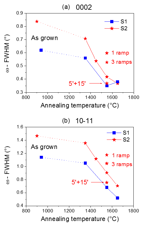
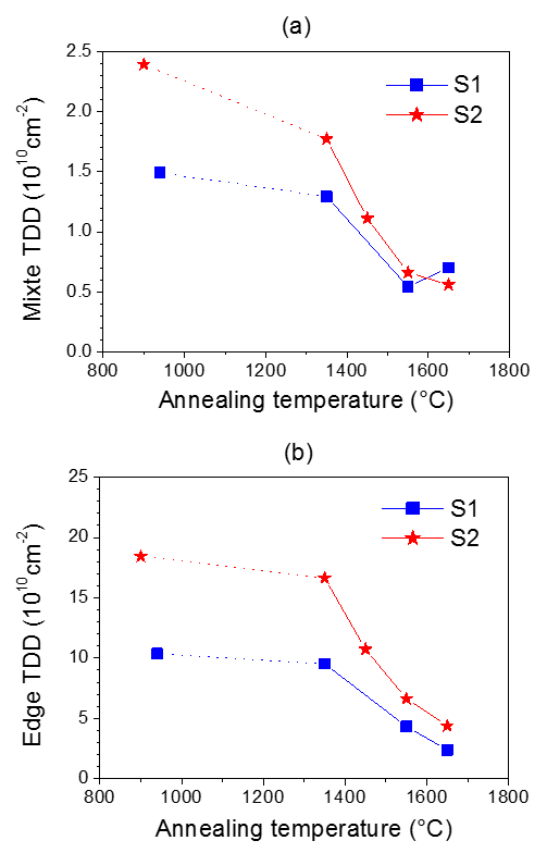
1) Evolution of mixed and corner dislocation densities of the annealing temperature of AlN (0001) layers epitaxially Sapphire (0001)
Rotation ω sample allows to put in condition of diffraction of atomic planes slightly disoriented, one in relation to others, because of the presence of defects in the layer. Therefore, the widths of the diffraction peaks according to ω, allow to evaluate the density of defects. In the example below, the mixed dislocation density (wedge) was calculated from the tilt (twist) determined using the Williamson-Hall method (Srikant).
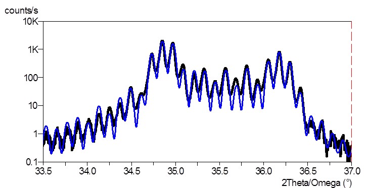
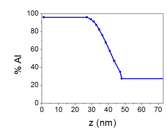
2) Determination of Al composition profile in a superlattice (AlN/Al0,3Ga0,7N)10
Simulation of the diffraction diagrams 2 θ / ω (to the left, blue curve) of a superlattice (AlN / Al0.3Ga0.7N)10 allows to determine the thickness of the super-network period as well as his composition profile (right). An interface layer to composition gradient is highlighted.
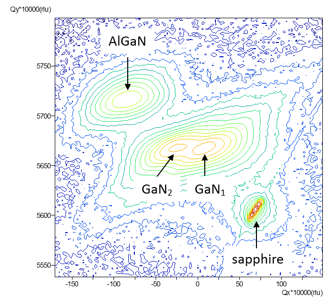
3) Mapping of reciprocal space around the line 11-22 of a hetero-structure composed of AlGaN / GaN / sapphire plane m
This measure makes it possible to quantify the disorientation of the layers relative to each other as well as to the substrate, and highlights the disorientation between the GaN MBE recovery layer and the underlying MOCVD GaN layer. Disorientations are included here between 0.6 ° and 1.6 °.
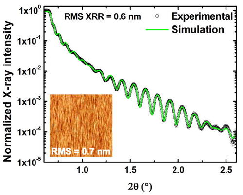
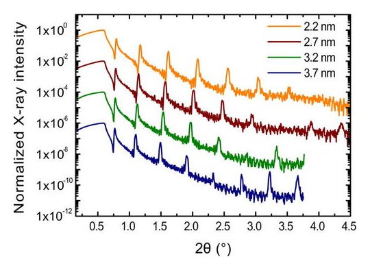
4) Reflectivity of epitaxial hetero-structures on ZnO plane m
Left: experimental and simulated reflectivity diagrams of a double barrier (Zn, Mg) O of 2.0 nm with a quantum well of ZnO of 4.0 nm. The thicknesses are deduced from the simulation. The composition Mg used for the simulation is 30%. RMS roughness determined by the simulation of the reflectivity diagram (RMS XRR = 0.6 nm) is consistent with that determined by AFM (RMS = 0.7 nm).
Right: the quantum multi-well reflectivity diagrams ZnO / (ZnMg) O for different well thicknesses. The thickness of the barrier is kept constant at 15.0 nm.
The devices used are described in the page characterization of CRHEA.