Highlights
Highlights 2020 (12/2020)
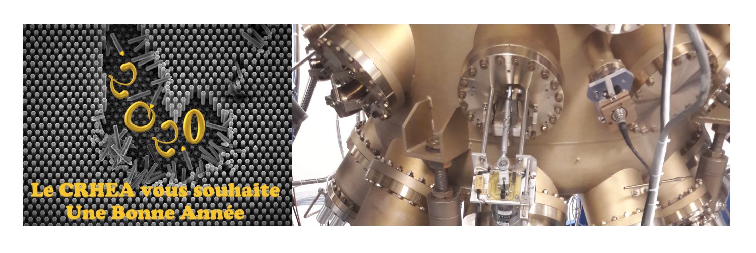
 CRHEA wishes you all the best for 2021.
The 2020 CRHEA highlights brochure is available.
☛ Read the content...
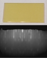
First 200 mm AlN-on-Si template using ammonia-based Molecular Beam Epitaxy (MBE) (06/2020)
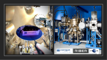
SOPHIA ANTIPOLIS, France, June 15th, 2020 – EasyGaN SAS, RIBER SA and the CRHEA-CNRS Laboratory reached an important milestone with the fabrication of a first 200 mm AlN-on-Si template using NH3-MBE. The joined team grew such a template with an unprecedented quality in terms of roughness, pit density and structural quality on an 8-inch Si wafer thanks to a RIBER MBE 49 reactor installed at the CRHEA laboratory.
High temperature operation of sublimated GaN nanowires (Applied physics letters – 06/2020)
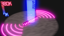
As part of an international collaboration between CRHEA and NTT (Japan), GaN nanolasers with a triangular section were produced by an original method of selective sublimation. The advantage of this method is that it does not damage the sides of the nanostructures as is the case with the use of conventional plasma etching.
Thanks to our approach, these nanowires show a laser emission far above ambient temperature. The article was selected to be featured on the cover of the June issue of Applied Physics Letters.
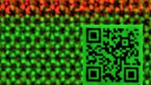
Quantitative imaging of metasurface holograms A new application of vectorial ptychography (Nature Communications - 05/2020)
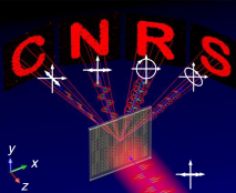
Metasurfaces are photonic components obtained by structuring
surfaces at a scale smaller than the wavelength of light. By generating
pixelated geometrical phase and/or polarization control properties,
they could revolutionize the design of ultra-compact 3D virtual
or augmented reality display systems. In order to control their
manufacturing, however, it is necessary to map all their optical
properties over areas of several hundred micrometers at the microscopic
resolution of their metapixels. Researchers from Institut Fresnel
(Univ. Aix-Marseille, CNRS, Centrale Marseille) and the Centre
de recherche sur l'Hétéro-épitaxie et ses applications - CRHEA
(Univ. Côte d'Azur, CNRS) have just taken this step, by reporting
quantitative images of a polarization-controlled meta-hologram.
This work is published in Nature Communications.
From measurements of diffraction patterns and their analysis by
phase retrieval algorithms, the researchers were able to reconstruct
a complete map of the optical properties of a meta-holograms displaying
an arbitrary patterns (here the CNRS acronym) with predetermined
light polarizations.
Magnesium nitride: a new semiconductor epitaxially grown (Physical Review Materials - 05/2020)
CRHEA has succeded in growing magnesium nitride epitaxially for the first time. Even if this material is known for more than a century and exploited as polycrystalline ceramics, it had never been obtained in its crystalline form. The access to high-quality Mg3N2 has enabled CRHEA to measure its fundamental physical properties: lattice parameter, linear thermal expansion coefficient and energy bandgap.
☛
Read more...
☛
Link to this topic on INP website...
☛ Dowload
file...
☛ This highlight will be publisled
in the newsletter "En
direct des labos" broadcasted every 15 days to the french
press
☛ It will also be relayed on
INP twitter account (@INP_CNRS)
Covid-19 : don ation of mmasks and gloves (03/2020)
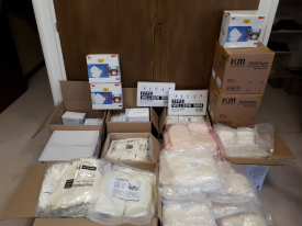
CRHEA donates its stock of masks and gloves to fight the Covid-19 epidemic.
A realistic wafer-level integration of metasurfaces with semiconductor lasers (Nature Nanotechnology - 01/2020)
 Ultra-thin flat optical structures, also called metasurfaces, offer
an innovative approach to controlling light. By integrating them
with vertical emission micro-lasers (VCSELs), they allow the creation
of arbitrarily programmable beam networks for imaging and telemetry
applications.
Ultra-thin flat optical structures, also called metasurfaces, offer
an innovative approach to controlling light. By integrating them
with vertical emission micro-lasers (VCSELs), they allow the creation
of arbitrarily programmable beam networks for imaging and telemetry
applications.Most importantly, the new degree of freedom offered by metasurface does not compromise the laser performances such as the operation mechanism, threshold, current distribution, lasing wavelength, high speed modulation, etc. This technique remains fully compatible with existing state-of-the-art VCSEL technologies, including the wafer-level fabrication process, the standard packaging process, electrical injection solutions and theoretical analysis. The arbitrary wavefront control directly at the wafer-level and the programmability of these devices would significantly promote applications in various wide-field applications, such as optical fibre communications, laser printing, smartphones, optical sensing, face recognition, directional displays and ultra-compact light detection and ranging (LiDAR).
☛ Paper link...
☛ Nature Blog link...
Highlights 2019 (01/2020)
 CRHEA wishes you all the best for 2020.
The 2019 CRHEA highlights brochure is available.
☛ Read the content...