
Scanning electron microscopy
Scanning electron microscopy allows structural, chemical, and luminescence analyses on samples produced in the laboratory or by our partners. When coupled with a writing device, this technique can also be used to perform electronic lithography steps for the manufacture of nanometric patterns. Two devices are operated by the CRHEACAM platform.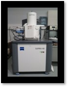
The Supra 40 is a very high-resolution Schottky gun emission scanning electron microscope (SEM) that provides very stable emission currents (4pA-20nA). It can be used to characterize nanometric objects.
Accelerating voltage from 100V to 30kV
Magnification from x12 to x300,000 and resolution up to 1nm at 20kV (WD = 5mm)
Apertures from 7.5 to 120µm
Probes: high-efficiency SE In-Lens, classic SE2 Everhart-Thornley type
5-axis motorized sample stage: X, Y=130mm, Z=50mm, T=-3-70°, R=360°
Maximum sample size: Ø=100 mm, h=20 mm
Patterning accessory: Raith ELPHY PLUS system for electron lithography
 (link to the text on electron lithography in the crheatech platform).
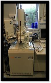
The JSM7000F is a high-resolution hot-tip (Schottky) field emission SEM. Its unique feature is its ability to achieve a high and very stable emission current of up to 100nA. It can be used to characterize objects at the nanometer scale.
Acceleratingvoltage from 500V to 30kV.Magnification from x12 to x100,000 and resolution up to 2.5nm at 5kV (WD=10mm).
Probes: classic Everhart-Thornley SE2 and a retractable AUTRATA BSE backscattered electron detector.
Motorized eucentric goniometric sample stage with 5 axes: X, Y=70mm, Z=40mm, T=-5-70°, R=360°
Maximum observable surface: Ø=80 mm, h=20mm
A SAMX X-ray energy dispersive spectrometry (EDX or EDS) microanalysis system. The X-ray detector is a 10 mm² SGX-Sensortech SSD (Silicon Drift Detector) with a sensitivity of 5 mV/keV.
This system can detect elements from Be onwards with a resolution of 133 eV and a speed of up to 150 kcps/s. It can be used to perform qualitative and quantitative analyses, elemental and quantitative spectral mapping, and phase analysis. - A GATAN MONO CL4 cathodoluminescence system, coupled with a liquid nitrogen-cooled stage
Sample preparation :
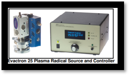
- an EVACTRON XEI Scientific RF plasma sample surface cleaning system that removes hydrocarbon contamination using plasma generated inside the microscope's observation chamber. This decontamination significantly improves image resolution
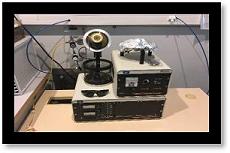
- an AGAR Scientific evaporator for preparing non-conductive materials, enabling the deposition of conductive layers: gold by plasma or carbon by evaporation.