The clean room includes all equipment and processes technologies (chemistry, photolithography, deposits, engravings, ...) intended the preparation of substrates and the manufacture of micro-components and optoelectronic. The realization of objects or devices of small size (micro- or nanometric) requires conditions essential cleanliness. In order to carry out these processes, it is therefore necessary to work in a controlled atmosphere area (particle rate, temperature, humidity and pressure). Upstream of epitaxy, optical lithography is used to structure substrates 1 to reduce stress in the realized structures and thus to limit the appearance of dislocations and cracks. After epitaxy, the clean room can be used to make 3D objects such as micro-drives 2 on which growth can be achieved again. Else motives with resolutions of the order of a few nanometers can be drawn with 3 electronic lithography, allowing in particular the realization of meta-surfaces. Finally, downstream of epitaxy, the clean room allows the realization of 4 devices micro- and optoelectronic devices such as high mobility transistors electronic and light-emitting diodes.
1) Structuring of substrates
Examples of structuring of the substrate by optical lithography,
before epitaxial growth.
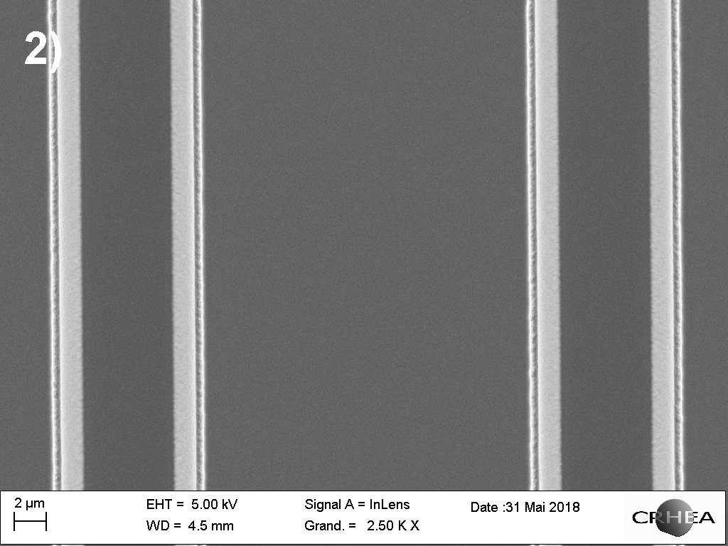
GaN or ZnO waveguides for integrated photonics are made on strips
(26 / 4µm) 1.7µm depth of ZnO substrate (figure. 1) or 7µm strips
of Si substrate (figure. 2).
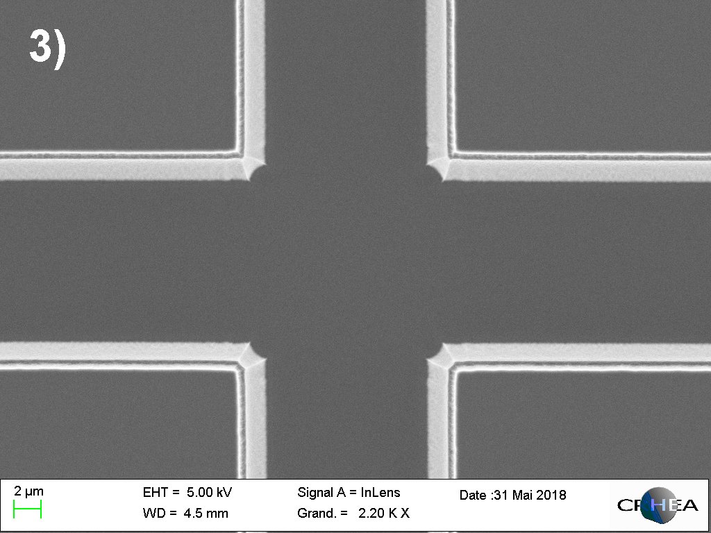
Figure 3: A Si substrate patterned in mesas 200µm * 200µm, spaced
from trenches of 10µm wide and 5µm deep.
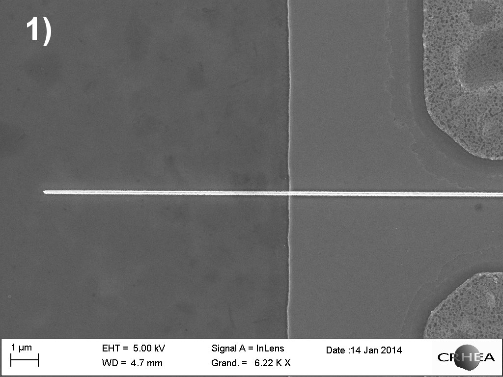
2) Realization of semiconductor micro-disks
The selective etching of hetero-epitaxial semiconductor thin films
allows the realization of micro-disks found in advanced micro- and
opto-electronic devices (MEMS and MOEMS).
Figure 1: SiC Micro-Disks on Si.
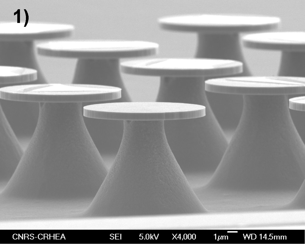
Figure 2: GaN epitaxy on AlN micro-disks, with the aim of developing
GaN facets semi-polar on silicon to produce LEDs emitting at a long
wavelength. The plans semi-polar GaN allow to incorporate more indium
than the polar planes and the structuration 3D of GaN eliminates extensive
stresses responsible for cracking epitaxial GaN layers on silicon.
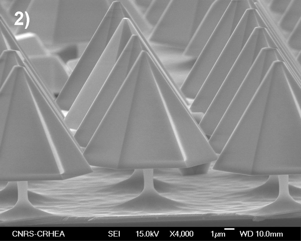
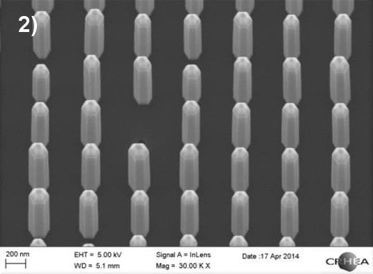
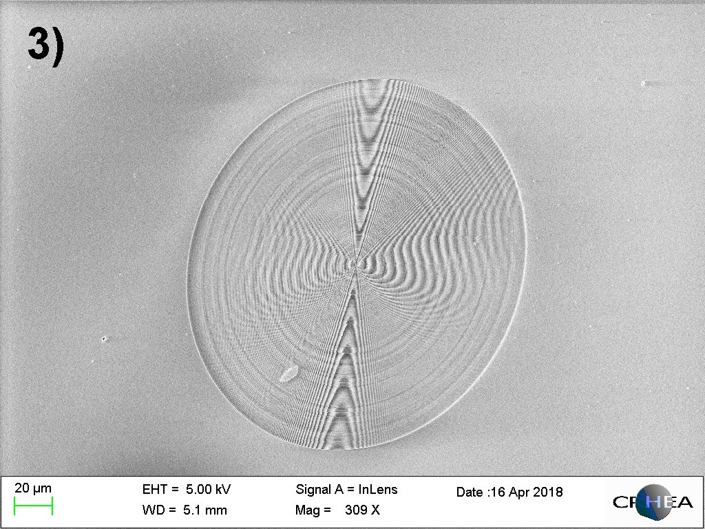
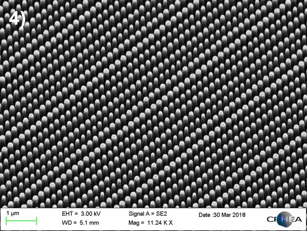
3) Electronic lithography
Electron beam lithography is a technique for drawing patterns with
resolutions of the order of a few nanometers, and to achieve objects
such as grids for high frequency transistors, nanoscale wires (better
crystalline quality as films), or meta-surfaces.
Figure 1: Grid from 100nm to 200nm of a GaN / AlGaN HEMT transistor.
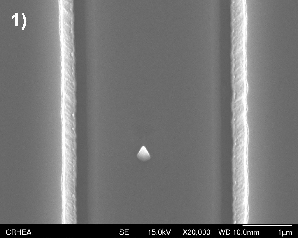
Figure 2: Growth of GaN nanowires with a patterned SiO 2
dielectric mask holes 100nm in diameter, spaced 500nm apart.
Convergent meta-lens of 200 .mu.m in diameter (figure. 3) based on
GaN piers from 50 nm to 100 nm in diameter (figure. 4).
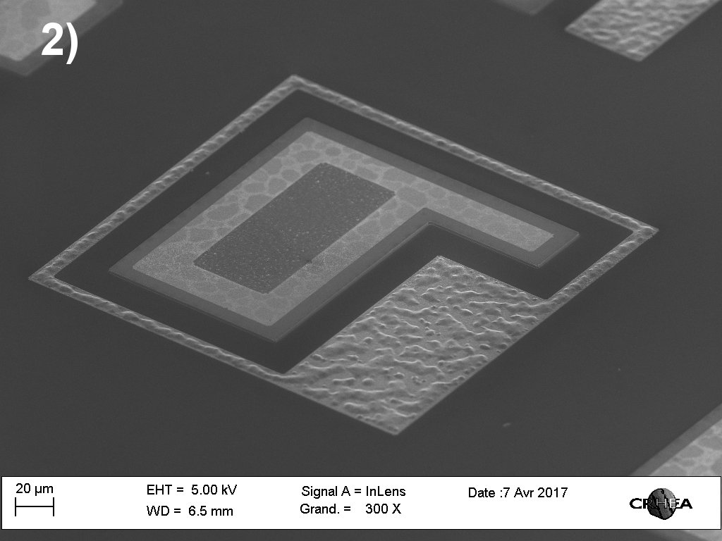
4) Realization of devices
The manufacture of devices, such as light emitting diodes (LEDs)
or HEMT transistors (High Electron Mobility Transistor), combines
steps of chemistry and photolithography (with alignment of several
levels of masks, physical-chemical plasma etching of mesas, deposition
of contacts by evaporation with electron gun, and heat treatments).
Figure 1: LEDs based on gallium nitride.
Figure 2: GaN / AlGaN HEMT. 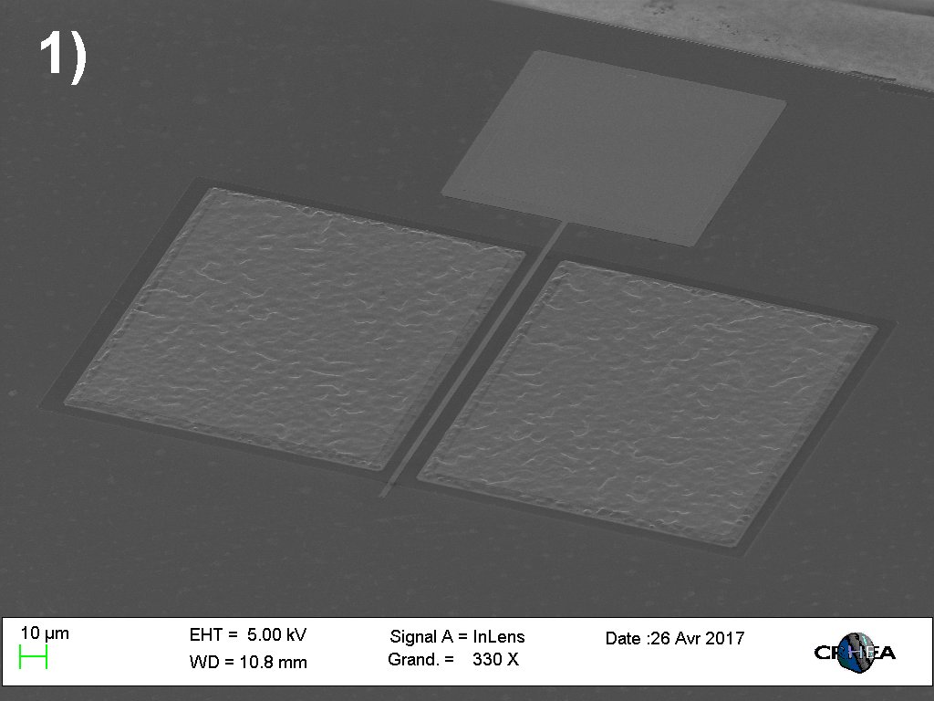
The devices used are described in the page technology platform of CRHEA.