Atomic Force Microscopy
Atomic force microscopy is used in the laboratory for the micrometric and nanometric scale characterization of semiconductor surfaces (nitrides of III elements (Ga, Al, In), SiC, BN, MoS2, etc.), conductors (NbN, graphene, etc.) and insulators (sapphire, MgO, etc.) studied in the laboratory by measuring the interaction forces between the atoms on the surface and the atoms at the tip of the microscope. The imaging mode mainly used in the laboratory is the intermittent mode (tapping mode TM).
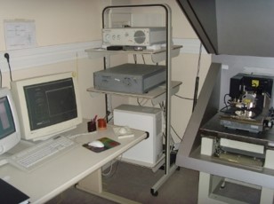
The CRHEACAM platform has two atomic force microscopes (AFM) manufactured by Bruker.
One is the Nanoscope IV Dimension 3100, which can image samples up to 4 inch in size with a surface scan ranging from 0.25 mm2 to 2500 mm2.
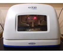
The other is the Dimension Edge, equipped with TM mode, which has similar characteristics to the Dimension 3100 and can study samples up to 8 inches in size without cutting. This non-destructive feature is beneficial for characterizing the surface of larger substrates, which are important for the development of a greater number of components.
AFM Dimension 3100 :
- Lateral resolution of 5 nm
- Vertical resolution of 10 pm
- TM mode characteristics:
- Stiffness constant (k) of 42 N/m
- Resonance frequency (f0) of 320 kHz
AFM Dimension Edge
- Lateral resolution of 5 nm
- Vertical resolution of 10 pm
- TM mode characteristics:
- Stiffness constant (k) of 42 N/m
- Resonance frequency (f0) of 320 kHz/li>
- Peak force ScanAsyst characteristics :
- Stiffness constant (k) of 0.4 N/m
- Resonance frequency (f0) of 70 kHz
Some AFM images
 AFM topographic image of a ScAlN semiconductor film on GaN AFM topographic image of a ScAlN semiconductor film on GaN, exhibiting exceptional
piezoelectric properties for RF electronics (transistors, filters) or power switching, which made it possible to determine the uniformity of
growth and low roughness (RMS = 0.3 nm).
AFM topographic image of a ScAlN semiconductor film on GaN AFM topographic image of a ScAlN semiconductor film on GaN, exhibiting exceptional
piezoelectric properties for RF electronics (transistors, filters) or power switching, which made it possible to determine the uniformity of
growth and low roughness (RMS = 0.3 nm).
 AFM topographic image of the surface of an AlN semiconductor layer AFM topographic image of the surface of an AlN semiconductor layer (thickness = 1 mm)
deposited on an AlN substrate (thickness = 200 nm) / sapphire, corresponding to the buffer layer for the development of UV LED structures,
which was used to identify and determine the dislocation density (d = 4.7 x 10⁹ dislocations/cm2).
AFM topographic image of the surface of an AlN semiconductor layer AFM topographic image of the surface of an AlN semiconductor layer (thickness = 1 mm)
deposited on an AlN substrate (thickness = 200 nm) / sapphire, corresponding to the buffer layer for the development of UV LED structures,
which was used to identify and determine the dislocation density (d = 4.7 x 10⁹ dislocations/cm2).
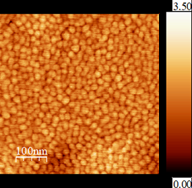
 AFM topographic image of MoS2 semiconductor flakes on GaN, which have great potential for use in FET transistors, photodetectors, and biosensors.
This image made it possible to determine the thickness of MoS2 to be approximately 0.7 nm, representing a single layer.
AFM topographic image of MoS2 semiconductor flakes on GaN, which have great potential for use in FET transistors, photodetectors, and biosensors.
This image made it possible to determine the thickness of MoS2 to be approximately 0.7 nm, representing a single layer.
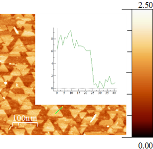
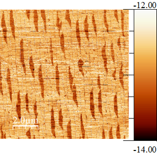 AFM phase image of graphene on SiC AFM phase image of graphene on SiC, used for the manufacture of quantum Hall effect resistance standards in
electrical metrology, revealing the non-uniformity of the surface hardness and therefore the presence of graphene monolayers and bilayers.
AFM phase image of graphene on SiC AFM phase image of graphene on SiC, used for the manufacture of quantum Hall effect resistance standards in
electrical metrology, revealing the non-uniformity of the surface hardness and therefore the presence of graphene monolayers and bilayers.