Power electronics
Compared to Silicon, wide bandgap energy semiconductors like GaN and SiC present major advantages to fabricate power switches (transistors) or rectifiers (diodes). Among them, one can cite the possibility to conduct larger current densities with lower electrical resistances in on-state (reduced losses) while sustaining larger voltages in off-state In this context, ELECTRO is hosting the SiC epitaxy activity of NOVASiC company and develops the epitaxy of Al(Ga)N/GaN HEMTs (High Electron Mobility Transistors) heterostructures on different substrates (Si, SiC, Sapphire, GaN, AlN ...). Of these substrates, Silicon is the one that concentrates most of efforts because of the prospects for large-scale industrial developments.
Transistors used as power switches have breakdown voltages which depend on the thickness and quality of the epitaxial layers on the silicon substrate. As can be seen below, these transistors show breakdown voltages that can exceed 700V in vertical configuration for a structure only 2 µm thick.
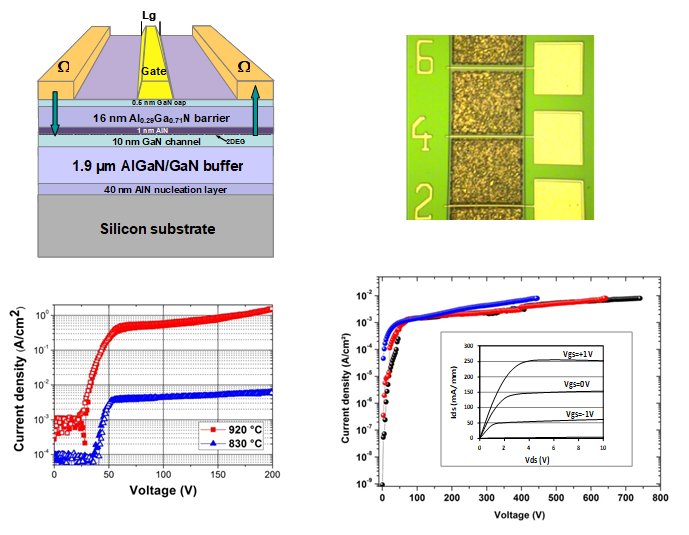
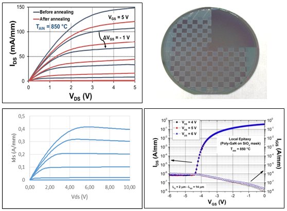
An important point right now is the development of "Normally-off" transistors, whether for power switches or for advanced telecommunications circuits. For this purpose, the laboratory develops original solutions based on local area epitaxy (collaborations with LAAS, LN2). The latter is also developed for the monolithic co-integration of GaN electron devices with Silicon C-MOS electronics (3)(4).
Main collaborations
IEMN, LAAS, LN2, GREMAN
References :
- Influence of AlN Growth Temperature on the Electrical Properties of Buffer Layers for GaN HEMTs on Silicon
- Growth of thick GaN layers on 4-in. and 6-in. silicon (111) by metal-organic vapor phase epitaxy
- Development of technological building blocks for the monolithic integration of ammonia-MBE-grown GaN-HEMTs with silicon CMOS
- Reduction of the thermal budget of AlGaN/GaN heterostructures grown on silicon: A step towards monolithic integration of GaN-HEMTs with CMOS