Highlights Electro
CRHEA in the GaN4AP european project (12/2021)

The GaN4AP project has the ambitious target of making GaN-based electronics one of the main components in a large spectrum of power converter systems, with the possibility of drastically cutting energy losses in power electronic systems, while ensuring high-frequency and higher power density operation. Thank to this joint effort a large variety of applications will benefit from a boost in performance, without sacrificing the system size and cost.
Record power density RF HEMT on GaN (2019)
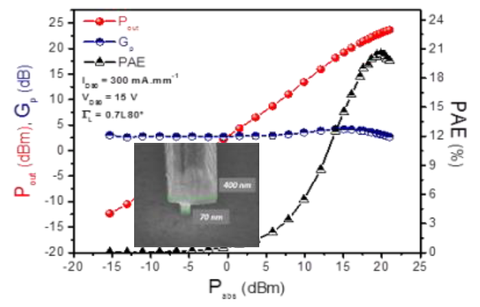 The development of performant and reliable GaN high-electron-mobility
transistors (HEMTs) on high crystal quality GaN is hampered by the
lack of large lattice matched substrates available at reasonable cost.
The development of performant and reliable GaN high-electron-mobility
transistors (HEMTs) on high crystal quality GaN is hampered by the
lack of large lattice matched substrates available at reasonable cost.
In this context, the growth of GaN HEMTs on commercial free-standing GaN substrates previously developed for high brightness light emitting diodes has been investigated as an alternative approach for high frequency applications.
Read more...
Thin channel GaN HEMT with 10 kV capability (2019)
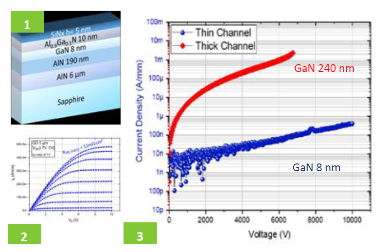 AlN is investigated as the basement of new highelectron-mobility transistors
(HEMTs) for high-power and high-voltage electronic applications.
AlN is investigated as the basement of new highelectron-mobility transistors
(HEMTs) for high-power and high-voltage electronic applications. Thanks to a very large band gap energy beyond 6 eV and high thermal conductivity, such semiconductor is very promising to overcome the limitations encountered with GaN based electron devices.
Read more...
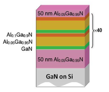
GaN RF HEMT structures grown by MOCVD on CVD 3C-SiC/Si (2018)
 Volume production of high performance GaN high electron mobility transistor
(HEMT) heterostructures on large diameter substrates is a key point
for the large scale development of high frequency telecommunications
like 5G.
Volume production of high performance GaN high electron mobility transistor
(HEMT) heterostructures on large diameter substrates is a key point
for the large scale development of high frequency telecommunications
like 5G. In spite of large availability of low cost Silicon substrates, the high surface reactivity and the large mismatch in crystal lattice parameter and thermal expansion coefficientwith GaN make the growth tricky.
Read more...
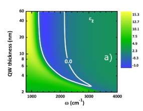
THz intersubband absorption in GaN based heterostructures grown on Silicon substrate (2018)
 AlGaN/GaN heterostructures present interesting features for optoelectronic
devices working in the TeraHertz (THz) range:
AlGaN/GaN heterostructures present interesting features for optoelectronic
devices working in the TeraHertz (THz) range:
- the possibility to build periodic heterostructures with energy levels separated with few tens of meV
- a large optical phonon energy which may enable the electron population inversion in quantum cascade lasers (QCLs) at room temperature
Read more...
Optical phase transition in semiconductor quantum metamaterials (2018)
 The direction of refracted light at an interface between two media
generally follows the conventional Snell-Descartes law.
The direction of refracted light at an interface between two media
generally follows the conventional Snell-Descartes law. Bystacking subwavelength-thick metallic and dielectric layers to form metamaterials, it is possible to realize unexpected behavior such as negative refraction.
Read more...