Harsh environments sensors
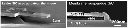
There is currently a strong demand, from many fields, for the realization of sensors capable of operating in harsh environments. The increased need to record the evolution of very specific chemical or biological media in real time is occurring in the medical field as well as in the automotive industry or the oil industry. The sensors must then be able to respond to environmental constraints that can be extreme. If the miniaturization of the sensors is widely developed (MEMS and NEMS) and allows today to position silicon sensors in very small spaces, thus becoming integrable on electronic chips, the choice of the material used remains crucial. Indeed, silicon sees its physical and electrical properties greatly degraded when the working temperature of the device is greater than 100°C. In addition, silicon has an increased reactivity in a biological medium, which severely handicaps it for use in a biological medium. With this in mind, a research theme of the Electro team is moving towards the evaluation of silicon carbide (SiC) as a basic material for developing sensors operating in aggressive media (1). Gallium nitride, already widely explored in other research topics, is also considered for this theme (2-4). The work developed focuses on the specific growth of these materials, the problems related to the growth process as well as their obtaining under architectures material potentially usable for the formation of structures forming the active elements of sensors: beams, membranes ... This axis relies on external collaborations (GREMAN laboratories, IEMN) as well as on national projects (currently: H2MEMS project - ANDRA funding 2017-2021, NEMSGaN 2019-2022 ANR project).
Main collaborations
GREMAN, IEMN
References :
- 3C-SiC – From electronics to MEMS devices
- Gallium Nitride as an Electromechanical Material
- AlGaN/GaN HEMTs with very thin buffer on Si (111) for nanosystems applications
- Influence of metal‐organic vapor phase epitaxy parameters and Si(111) substrate type on the properties of AlGaN/GaN HEMTs with thin simple buffer