Presentation of the Semipolar activity
In nitride heterostructures grown along the polar c-axis, the presence of polarization discontinuities greatly modifies the band structure. In the case of LEDs, the strong (several MV/cm) polarization fields in the quantum wells are detrimental for the quantum efficiencies, especially when high indium concentration and/or large QW width are employed in order to push the wavelength emission towards the green. This effect, known as the quantum confined Stark effect (QCSE), can be almost suppressed when the c-axis forms an angle Θ with the growth direction of the LED. Such orientations are called semipolar (0 < Θ < 90°) or non-polar (Θ = 90°). Growth of high quality semipolar and non-polar GaN by heteroepitaxy on sapphire or silicon is very challenging and invariantly gives rise to a large number of stacking faults (SFs ~ 106 cm-1) and threading dislocations (TDs ~ 1010 cm-2). A very promising approach for defect reduction is the selective growth from the inclined c-facets of an etched sapphire surface on which inclined GaN polar growth along [0001] takes place. In the present case, we use a chemically-etched stripe patterned r-sapphire, although the same technique was also adopted for Si or SOI (Silicon On Insulator). The different growth steps are summarized in figure 1.
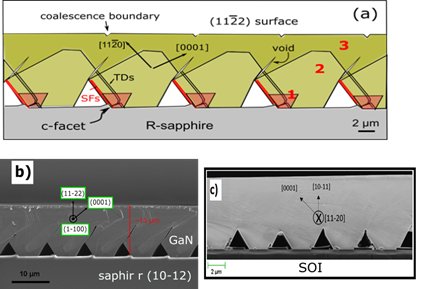
This method gives rise to low defect semipolar nitride substrates suitable for the realization of semipolar optoelectronic devices such as visible LEDs emitting at long wavelength (yellow/red) or QCD (quantum cascade detector) operating in the terahertz range.