GaN / Si Nanophotonics
Based on the expertise acquired in the last 20 years in the field of epitaxy of nitride elements III on silicon substrate, we take up a new challenge: Combining the remarkable properties of nitrides III elements with the extraordinary maturity of technological processes on silicon, to manufacture new and innovative objects in nanophotonics in the UV-visible-near IR range.
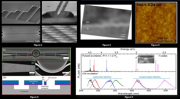
The main approach we develop to achieve these objects is to manufacture suspended membranes to eliminate the absorption of silicon. Indeed, it turns out that there is a high selectivity of etching between the silicon and nitrides III elements and thus the manufacture of suspended membranes is relatively simple (Figure 1). For these membranes to have interesting properties, it is generally necessary for their thickness to be of the order of the wavelength (Λ) of the photons that it is desired to generate and / or propagate. Thus, typically, the silicon epitaxial element III nitride layers must be relatively thin, of the order of 100 and 500 nm. The heteroepitaxy of thin layers as thin with interesting optical properties is a real challenge. Indeed, to obtain a good quality material it is generally necessary to epitaxize several microns of material on silicon in order to filter a part of the structural defects generated at the interface Si / element III nitride. Therefore, upstream of the production of the suspended membrane, there is a critical work to be done on the material during the epitaxial phase, which consists in having a Si / nitride element III interface that is as perfect as possible (Figure 2) quickly obtain an extremely smooth growth front (Figure 3). The density of defects and the stress in these thin layers are also critical points. Once these aspects are optimized, we have the choice to insert or not active zones (quantum wells, quantum dots, bidimensional electron gas, ...) depending on whether we want to manufacture lasers, waveguides , resonators, modulators or generate non-linear effects, frequency combs ...
After the epitaxial phase carried out at CRHEA, the electronic lithography manufacturing step is followed by a silicon under-etching step, which makes it possible to release membranes and to make microdisks, photonic crystals, waveguides, or even to couple these different objects (Figure 4). These manufacturing steps as well as the specific studies that are conducted on these objects are mainly carried out by our partners (Figure 5).
Some examples of achievements:
- Blue Microlasers integrated on a photonic platform on silicon ACS Photonics (2018)
- Deep-UV nitride-on-silicon microdisk lasers SCIENTIFIC REPORTS Vol. 6, 21650 (2016)
- III-Nitride-on-silicon microdisk lasers from the blue to the deep ultra-violet APL 109, 231101 (2016)
- Phase-matched SHG with on-chip GaN-on-Si microdisks SCIENTIFIC REPORTS 6, 34191 (2016)
- Near-infrared III-nitride-on-Si nanophotonic platform with µdisk resonators OPTICS EXPRESS 24, 9602-9610 (2016)
- Resonant SHG in a gallium nitride two-dimensional photonic crystal on silicon APL 106, 081105 (2015)
- Near-infrared gallium nitride two-dimensional photonic crystal platform on silicon APL 105, 011104 (2014)
- High quality factor AlN nanocavities embedded in a photonic crystal waveguide APL 100, 191104 (2012)
- High quality factor photonic resonators for nitride quantum dots PSS b 249, 449-454 (2012)
- AlGaN-on-Si-Based 10-µm Pixel-to-Pixel Pitch Hybrid Imagers for the EUV Range EDL 32, 1561-1563 (2011)
- High Q nitride-based optical cavities: µdisks with embedded
GaN/Al(Ga)N QDs OPTICS LETTERS 36, 2203 (2011)