Perovskites
- Halogenated Perovskites, have emerged over the past 10 years as a new generation of semiconductors offering exceptional potential for
a wide range of optoelectronic applications (LEDs, lasers, photodetectors, transistors, but also in fields such as quantum optics and spintronics).
- In the SENS team, we are primarily interested in the potential of these materials for solar applications. Perovskite-based solar cells
are based on polycrystalline materials deposited by low-cost methods, which nevertheless show record efficiencies of over 25% (30% in tandem with Si).
Improving crystalline quality by epitaxial growth of halogenated perovskites using EJM, aims to increase the efficiency of solar cells and of
course to learn more about the optoelectronic properties of these materials.
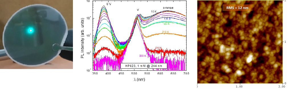
- Our study material is CsPbBr3. To get around the problem of using Br, we use CsBr and PbBr2 binary sources. We first validated the congruence
of evaporation of these binaries in EJM, which normally uses elemental sources. This represents a major technological advance.
- We are currently focusing on optimizing the structural quality of the ternary material synthesized. Despite a Pb deficit in the composition compared
with CsPbBr3, the material emits intense green luminescence around 510nm (2.43 eV), but also shows a luminescent band around 3.2 eV. In view of all
the optical and structural studies carried out so far, we believe that we have CsPbBr3 perovskite crystals in a poorly crystallized CsBr matrix.
 Contact ?