Highlight SENS
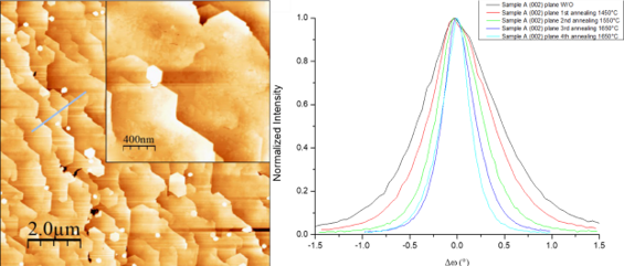
- AlN growth on h-BN for UV LEDs
To obtain efficient UV LEDs, approaches are being studied to optimize the growth of the AlN material used in LED structures, as bulk AlN crystals are very expensive and small in size. In collaboration with Georgia Tech-Lorraine, we are working on the growth of AlN on hexagonal boron nitride (h-BN), a 2D material characterized by weak out-of-plane van der Waals (VDW) bonds. By taking advantage of this property, h-BN layers could be used as a mechanical separation layer to exfoliate UV LEDs for transfer to conductive substrates for the realization of high-efficiency devices. In this study, the role of annealing, carried out at high temperature (≥ 1450°C), on AlN crystalline quality and surface morphology was investigated as a function of AlN thickness, annealing time and temperature. Optimum conditions were identified for fabricating AlN/h-BN templates.
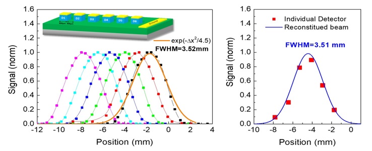
- GaN detector for protontherapy
Proton beam control improves and accelerates proton irradiation for cancer treatment. Longer-term applications include proton imaging as a replacement for X-ray imaging. We demonstrate here that an array of 6 GaN diodes can measure the proton beam shape with a spatial resolution given by the detector size. An improved configuration allows us to reduce noise and measure lower proton currents. We demonstrate here that a current density of 1pA/cm2 can be detected with an 800µm wide GaN pin diode. An integration time of 1s should make it possible to measure current density down to 0.1pA/cm2, the level required for proton imaging.
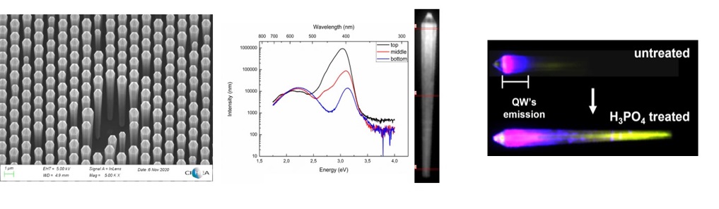
- Towards homogeneous luminescence along GaN/InGaN core-shell nanowires
As part of a project to develop flexible nanowire LEDs, we have studied the distribution of the InGaN shell along a single GaN nanowire. Using cathodoluminescence and transmission electron microscopy, we demonstrated the formation of a SiGaN passivation layer at the interface between the GaN core and the shell, and observed the degradation in quality of InGaN quantum wells epitaxial to this layer. We explored the possibilities of eliminating this by ex-situ and in-situ etching. After chemical treatment, we succeeded in obtaining nanowires entirely covered by the InGaN layer. This enables visible emission to be obtained along the entire length of the nanostructures, improving on the standard coverage reported in the literature.