UV micro-emitters for wireless underwater optical communication without direct line of sight

Effective communication between objects is crucial for underwater research and development. By creating UV micro-emitters based
on aluminum gallium nitride (AlxGa1-xN) with wavelengths between 300 and 320 nm, it is possible to increase light diffusion, reduce
solar radiation noise, and increase data throughput.
The development and operation of an original 3D microarchitecture made of AlxGa1-xN micro-platelets will enable the creation of more efficient devices.
High-quality InGaN templates for red µLEDs

The external quantum efficiency of red InGaN-based LEDs is currently below 5%, whereas it exceeds 80% in blue. One reason for this low efficiency is the significant lattice parameter mismatch between GaN and InxGa1-xN with a composition x close to 40%, which is necessary to achieve red emission. This parameter mismatch leads to the formation of structural defects that are detrimental to radiative efficiency. To overcome this challenge, the fabrication of high-quality InyGa1-yN templates is being considered. We are currently developing an approach based on the porosification of InGaN layers through sublimation.
GaN semi-polar MicroLEDs for display

The semi-polar GaN has the potential to increase high-current efficiency, incorporate more Indium for emissions at longer wavelengths (e.g., green and red), and produce polarized light, which is beneficial for many display applications. Growing GaN on textured SOI substrates aims to create a network of microLEDs localized in regions of high structural quality.
MicroLEDs based on GaN patches on SOI
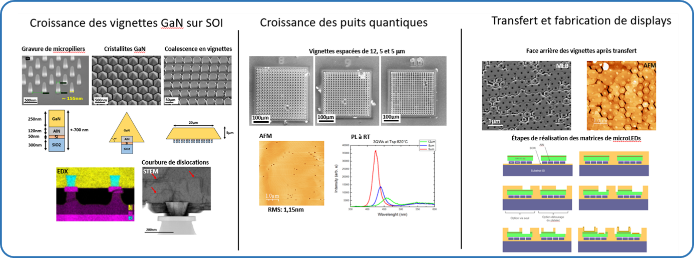
The principle of the PEGADIS project is to create a microLED matrix based on high-quality crystalline GaN vignettes on SOI pillars. The idea is to take advantage of the creep properties of SiO2 at the GaN growth temperature to reduce the dislocation density during the coalescence of GaN crystallites. Another benefit of this approach is the ability to produce microLEDs without resorting to post-growth etching techniques. These are known to cause a decrease in luminescence efficiency when device sizes are on the order of a few micrometers.