| Recent publications
|
|---|
⋄ Etching of the SiGaxNy Passivation Layer for Full Emissive Lateral Facet Coverage in InGaN/GaN Core–Shell Nanowires by MOVPEJulien Bosch, Pierre-Marie Coulon, Sébastien Chenot, Marc Portail, Christophe Durand, Maria Tchernycheva, Philip A. Shields, Jesús Zúñiga-Pérez, Blandine Alloing |
⋄ Pendeo-epitaxy of GaN on SOI nano-pillars: Freestanding and relaxed GaN platelets on silicon with a reduced dislocation densityR. Dagher, P. de Mierry, B. Alloing, V. Brändli, M. Portail, B. Damilano, N. Mante, N. Bernier, P. Gergaud, M. Cottat, C. Gourgon, J. Zúñiga-Pérez, G. Feuillet |
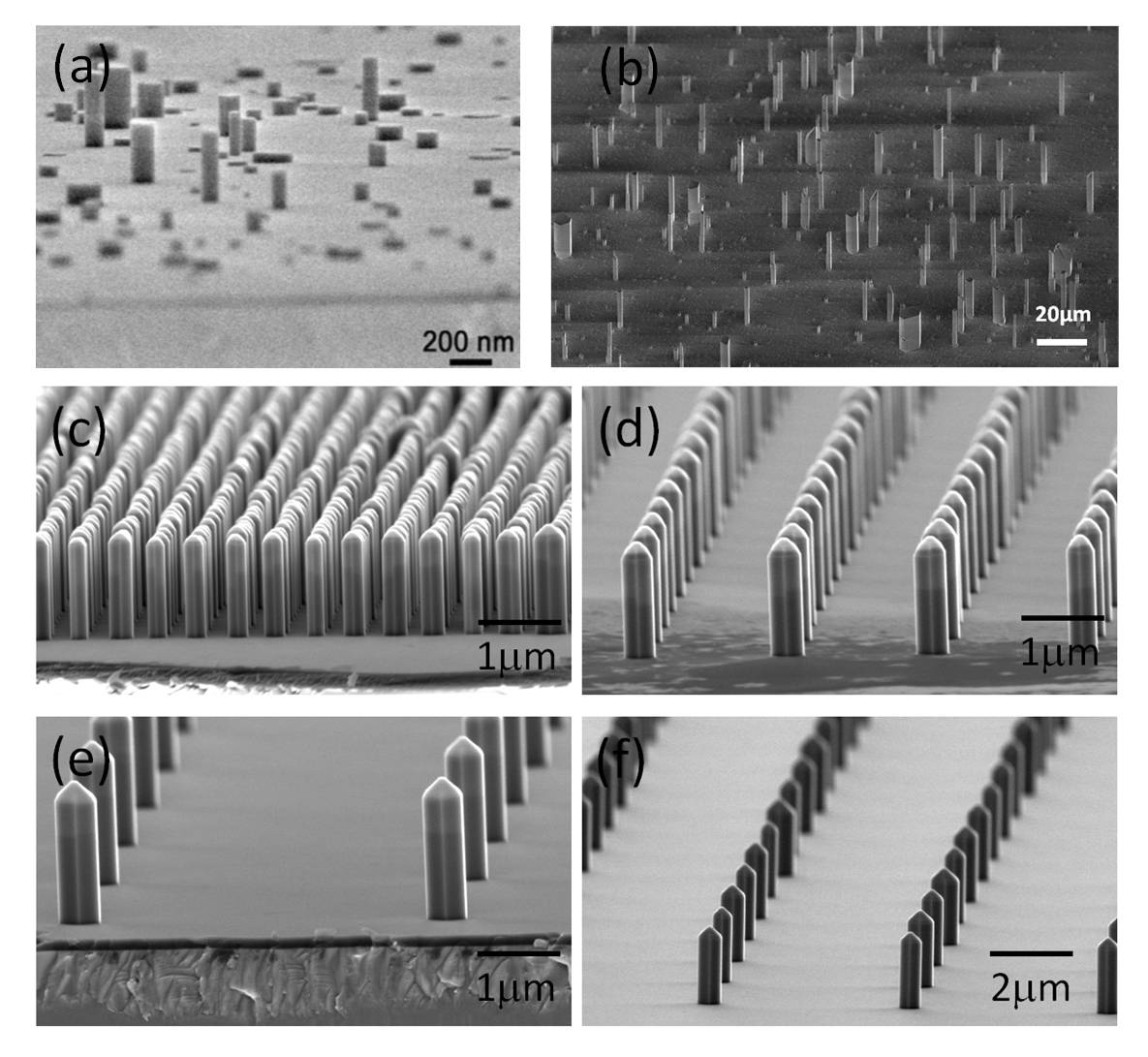
GaN nanowires are becoming increasingly popular due to their remarkable structural and morphological properties. These nanostructures first have free lateral surfaces that allow effective relaxation of the stress. They thus have a very low density of structural defects in comparison with the GaN planar layers. The presence of defects is a factor limiting the effectiveness of nitride-based devices. In addition, the one-dimensional geometry enhances light extraction and absorption efficiency. Finally, the manufacture of radial or "core-shell" heterostructures makes it possible to obtain a larger volume of light emission with respect to a planar heterostructure for the same substrate surface, as well as to increase the incorporation of Indium. All these qualities make GaN nanowires particularly interesting for the realization of optoelectronic devices such as LEDs, LASERs and solar cells. Nanowires also have their place in the field of sensors, because their large surface-to-volume ratio gives them a high sensitivity of detection and a better response time. Different types of sensors based on GaN nanowires have thus been realized: gas sensor, biochemical sensor, pressure sensor, etc.
Figures 1a and 1b below show the nanowires made by CRHEA by EJM with ammonia source as well as by MOCVD, in self-organized growth mode. In the interest of a better homogeneity and a better control of their positioning, the localized growth of nanowires on dielectric mask was then developed by MOCVD, as shown in Figures 1 (c), (d), (e) and F). The optimization of the nanowires manufacturing process as well as the study of their structural and optical properties were the subject of a first thesis defended in 2014 by Pierre-Marie Coulon. Another thesis in progress is devoted to the realization of an electrically injected polariton laser based on GaN microfilts, within the framework of the LABEX GANEX.