Contacts:
B. Damilano(coordinator) webmestre
Home > Overview
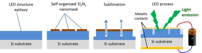
Efficient (Ga,In)N light emitting diodes can be grown on Si substrate but this requires the use of thick and complex buffer layers (several micrometers) which is a bottleneck for the massive adoption of the Si as a substrate for the epitaxy of nitride semiconductor materials. In NAPOLI we propose to use the simplest possible buffer layer and to improve the material quality after growth by a porosification process based on selective area sublimation.