
Main results
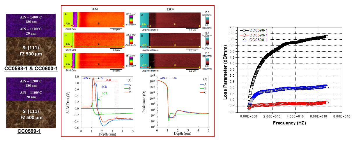
The first main result is the identification of the origins of microwave propagation losses and the development of solutions to mitigate them in the context of MOCVD growth. As illustrated bellow, scanning capacitance microscopy (SCM) and scanning spreading resistance microscopy (SSRM) performed on beveled MOCVD grown AlN-on-Si evidenced the presence of a conductive p-doped channel in the Silicon substrate. The comparison of samples A (CC0598), B (CC0599) and C (CC0600) confirms the primary role of the growth temperature (here maximum setpoint was 1200°C or 1400°C) as well as the reactor history on the channel thickness, resistivity and resulting RF propagation losses. Secondary ion mass spectrometry indicated that diffusion of residual Gallium was responsible for the doping of the substrate.
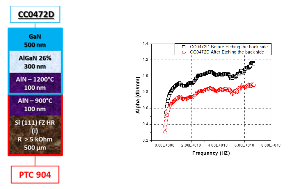
A second important result is the demonstration of the interest of new intermediate layers of materials deposited with other techniques. The first alternative consists of AlN nucleation layers grown at noticeably lower temperature, typically around 900°C by molecular beam epitaxy (MBE). Compared with MOCVD, such nucleation layers present better crystal quality without inducing a parasitic channel in the Silicon substrate. Sheet resistance superior to 20 kOhm/sq can be achieved and GaN buffer layers regrown by MOCVD on such template produced RF propagation losses below 0.8dB/mm at 40 GHz.
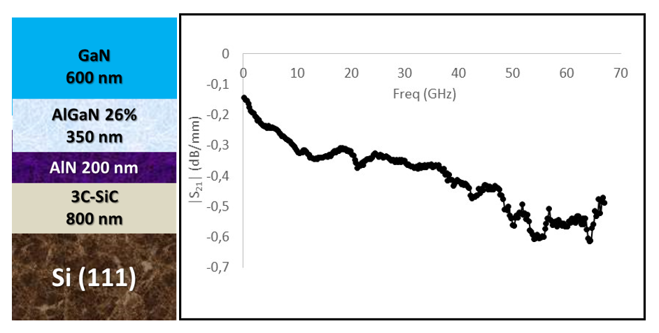
The most efficient alternative we developed is the one based on cubic SiC (3C-SiC). Cubic SiC was grown by CVD on Silicon. Sheet resistance superior to 20kOhm/sq and propagation losses below 0,4dB/mm at 40 GHz were obtained with such templates. Such electrical properties were preserved after the MOCVD regrowth of GaN buffer layer including AlGaN and AlN nucleation layers.
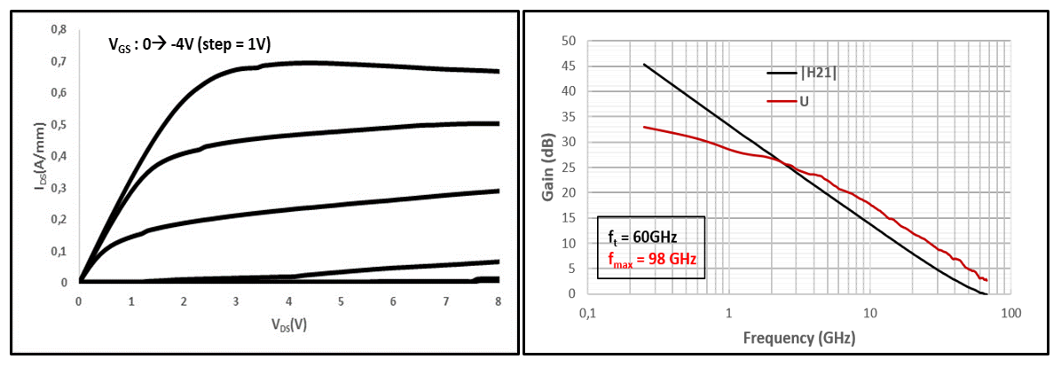
Furthermore, transistors fabricated with 75 nm gate on an AlGaN/GaN HEMT heterostucture grown on such template exhibited a safe high frequency behavior with maximum operation frequency close to 100 GHz.
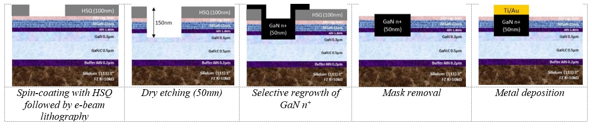
Last, an original process based on the e-beam lithography of HSQ resist has been developed to define the local area regrowth windows of highly doped GaN contacts on HEMT structures. The regrowth performed with MBE produced very well defined ohmic contacts with resistance below 0.35 Ohm.mm without the need of high temperature annealing.
Scientific outcomes
- Critical role of AlN growth temperature and advantage of using MBE for nucleation layer growth: Yvon Cordier et al, Physica Status Solidi A 2017, 1700637;
- Advantage of cubic SiC for MOCVD growth of GaN HEMTs on Silicon (collaboration with NOVASiC): Eric Frayssinet et al, Phys. Status Solidi A,2020, 1900760;
- Evidences of Silicon p-doped channel at AlN/Si interface: Micka Bah et al, Scientific Reports, (2020) 10, 14166.