High frequency electronics
GaN-based electron devices are key elements for the development of broadband wireless telecommunications. Indeed, the combination of large breakdown electric field (approximately 4MV / cm) and electron transport properties like mobility and velocity make GaN electron devices very promising candidates for high frequency applications (several GigaHertz), especially for base station emitters. In this context, CRHEA is developing the of epitaxy of Al(Ga)N/GaN HEMTs (High Electron Mobility Transistors) heterostructures on substrates like Si, SiC, Sapphire, GaN, AlN... In a same way as for power electron devices, Silicon is the substrate that concentrates most of efforts because of the prospects for large-scale industrial developments.
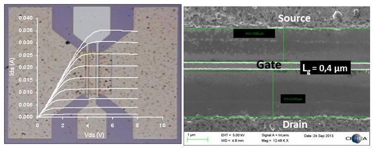
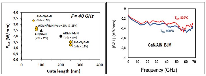
To reduce manufacturing costs, wireless telecommunications systems require amplifiers able to deliver large power densities at high frequencies. Power densities that can exceed 3 W / mm at 40 GHz have been demonstrated. In addition, propagation losses as low as 0.3 dB / mm at 40 GHz allow to consider the fabrication of efficient monolithic circuits (MMICs). In this context, the ASTRID GoSiMP ANR project was devoted to the study of the MOCVD growth of HEMTs GaN structures on Silicon.
Main collaborations
IEMN, LN2, GREMAN, NOVASiC, EasyGaN
References :
- Al(Ga)N/GaN high electron mobility transistors on silicon
- Influence of AlN Growth Temperature on the Electrical Properties of Buffer Layers for GaN HEMTs on Silicon
- MOVPE growth of buffer layers on 3C-SiC/Si(111) templates for AlGaN/GaN High Electron Mobility Transistors with low RF losses, Phys. Status Solidi A,2020, 1900760
- Electrical activity at the AlN/Si Interface: identifying the main origin of propagation losses in GaN-on-Si devices at microwave frequencies, Scientific Reports, (2020) 10, 14166.