
Objectives
The main goal of the project is to establish a complete processing chain able to produce high power density, good efficiency HEMT transistors operating at 40 GHz and beyond on low cost Silicon substrates. The hetero-epitaxial growth of GaN based heterostructures, the first step of the processing chain, will have to rely on MOCVD, the most industrial growth technique in the field to ensure large scale production and cost reduction. More, compared with components operating below 30 GHz approximately, the processing will have to be noticeably modified due to the necessity to enhance the charge control within short gate transistors and to reduce access resistances dramatically impacting the device performance at high frequencies. Therefore, the project will address both crystal growth and device process issues.
These issues are analyzed hereafter and the envisaged solutions for tackling them will define the work program of the present proposal.
Low RF losses in the buffer/substrate
The first issue concerns the epitaxial growth of the buffer layer on Silicon. The main goal will be to develop a buffer compatible with high frequency operation and high efficiency transistors, namely buffer with low microwave propagation losses, low trap density and high crystal quality. If highly resistive Silicon is available, it appears that growing GaN/AlN materials can noticeably degrade the resistivity and microwave propagation, especially with high-temperature growth techniques like MOCVD. First, the project will address this issue by focusing on the Achilles heel of the material system, i.e the interface between the nucleation layer (AlN) and Silicon.
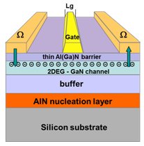
Low resistance channel with thin barrier
The following objectives will be to demonstrate high quality High Electron Mobility Heterostructures on top of such optimized buffer layers and to fabricate high power density and high efficiency transistors for frequencies of 40 GHz and beyond. To do so, Al-rich thin barriers composed of AlGaN or InAlGaN will have to be grown by MOCVD on top of the buffer layers with a sheet resistance as low as possible (<300 Ohm/sq). In-situ grown SiN, GaN or AlN capping are envisaged solutions as a first passivation aiming to protect the Al rich barrier during the device process and to reduce the impact of surface traps.
Enhanced confinement of the carriers in the channel
The necessary reduction of the gate length to reach high frequency of operation exacerbates short channel effects. To avoid the punch-through of electrons, the buffer layer will have to contain a back-barrier able to confine them into the channel. Thick AlGaN or thin AlN barrier will be tested.
Reduced source resistance
For operation at 40 GHz and beyond, not only the gate length will have to be reduced below 100 nm while keeping a good electron confinement, but the access resistances in transistors need to be drastically lowered well below 1 Ohm.mm. With sheet resistances of the order of 300 Ohm/sq, the solution for lowering the source resistance is to reduce as much as possible the distance between the source contact and the gate. This can be easily achieved with the present lithography techniques, for instance with electron beam lithography. However, the high temperature (T>800°C) thermal annealing of metals deposited for ohmic contact formation leads to some metal fusion with a loss of definition of the edges. This makes difficult to achieve contact spacing below 0.3 µm. In order to reach such a goal, highly doped GaN will have to be selectivity regrown in windows opening after etching the barrier material. For this purpose, MBE growth technique will be preferred due to the lower growth temperature compared with MOCVD. The aim of this approach is both to reach low contact resistances and to avoid the metal high temperature thermal annealing detrimental to the reduction of device dimensions. Ultimately downscaled devices can be envisaged using the top of the gate as a mask for self-aligned contacts.