Navigation: home > problem and objectives
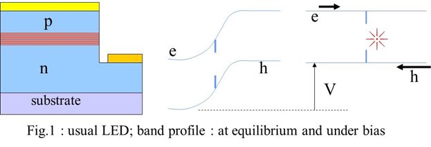
Let us first briefly recall how the LED works (Fig. 1). A semiconductor structure is grown with an n type layer, then a quantum well (QW) region, and finally a p type region. Under forward bias, electrons and holes are injected from the contact layers into the QW, recombine, and emit light. Many phenomena occur in series in the LED: carriers must be injected in the emitting region (ηinj), they must recombine radiatively (IQE), and the photon must be extracted out of the material (?ext), so that the external quantum efficiency (EQE), which is the ratio between the number of emitted photons and the number of injected electrons, is given by EQE=ηinj ×IQE × ηext.
The wall plug efficiency (WPE), figure of merit for the consumer, is the ratio of the optical power to the electrical power. Then, WPE=EQE x hν/eV. In ideal LEDs, the bias V is comparable to the photon energy hν (in units of e), so that WPE ≈ EQE. In non-ideal LEDs, for instance with large access resistances, the bias V is larger than hν by a quantity ΔV, and WPE≈EQE x hν/ (hν+ΔV). In order to maximize the WPE, one must maximize the EQE and minimize ΔV.
Nitride (AlGaInN) based LEDs are used in the visible range as monochromatic sources for displays and as white sources for solid state lighting. In the visible range, these LEDs are already very efficient (EQE of 80%) at least at moderate currents (≈10 A/cm2) and operate at a low bias of 3 V or so, which is the value expected from the band gap value of the emitting material (about 3eV). When moving to the UV, the band gap energy of the emitting material increases and the operating bias of UV LEDs is expected to increase accordingly. For instance, the transition energy of a quantum well emitting at 275 nm is about 4.5 eV and the operating voltage is expected to be about 4.5 V. However, nitride LEDs emitting in the UV are either operated at a larger bias or suffer from a low light output (external quantum efficiency typically of a few %). These problems, and the resulting trade off, is due to the difficulties in p doping AlGaN materials. The shorter the wavelength, the larger Al content in AlGaN and the more difficult the p doping. This induces two problems. First the hole injection is poor leading to a low radiative efficiency (small EQE). Second, the access resistance to the p side increases, the total bias increases, which reduces the wall plug efficiency. It also induces current spreading issues and light emission non uniformities. The usual solution is to use GaN layers on the p side (at least in part of it) in order to limit the degradation of the electrical behaviour. However, these GaN layers absorb UV light, which reduces the light extraction and the EQE, and thus also reduces the wall plug efficiency. Best UV LEDs emitting at 275nm have EQEs in the range of 10% and operating biases around 10V, leading to WPE around 5%. In order to go beyond this compromise and above the associated typical 5% WPE value, one has to propose novel approaches.
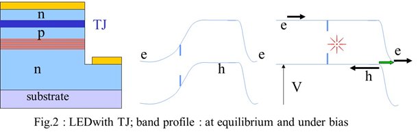
The tunnel junction (TJ) is a highly doped pn junction. The depletion region is very narrow and can be crossed through tunnel effect by carriers. Electrons are injected from the conduction band (CB) to empty states in the valence band (VB), or from filled states in the VB towards empty states in the CB. As a result, an electron current in the n side is transformed into a hole current in the p side. Inserting such a TJ on the p side of a LED leads to a device with two n type contacts (Fig. 2). As an advantage, the top contact layer becomes n type, with a low resistivity. The metal has a low contact resistance and current spreading is good. This is of particular interest for AlGaN materials. The price to pay is a voltage drop across the tunnel junction. Our project consists in developing such TJs for UV LED and minimizing the voltage drop across the TJ.
The general objective is to reach a TJ resistance lower than 10-3 Ωcm2, an absorption in the TJ lower than 2%, leading to a WPE of 1% for an LED emitting at 275 nm.